

Photodiodes are semiconductor devices responsive to high energy particles and photons. Photodiodes operate by absorption of photons or charged particles and generate a flow of current in an external circuit, proportional to the incident power. Planar diffused silicon photodiodes are P-N junction diodes. A P-N junction can be formed by diffusing either a P-type impurity, such as Boron, into a N-type bulk or epitaxial silicon wafer, or a N-type impurity, such as Phosphorus, into a P-type bulk or epitaxial wafer. The diffused area defines the photodiode active area. To form an ohmic contact, another impurity diffusion into the backside of the wafer is necessary. The active area is coated with an Anti-Reflection coating to reduce the reflection of the light for a specific predefined wavelength. The P and N-sides of the junction have metal pads, which make an electrical contact through dielectric layers.
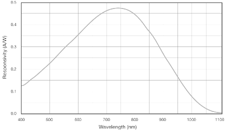
The typical spectral response curves of Silicon photodiodes are shown in Figure,
Electrical Characteristics A p-n junction photodiode can be represented by a current source in parallel with an ideal diode. The current source represents the current generated by the incident photons, and the diode represents the p-n junction. In addition, a junction capacitance Cj and a shunt resistance Rsh are in parallel with the other components. Series resistance Rs is connected in series with all components in this model.
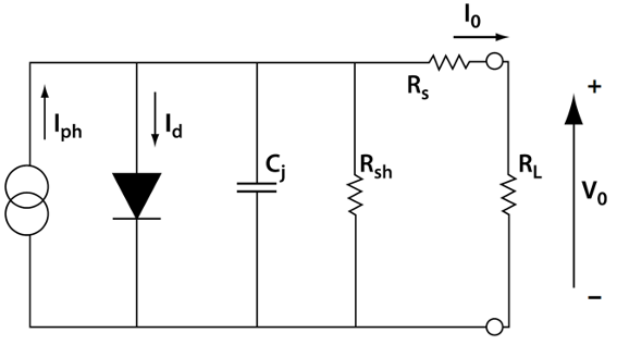
Shunt Resistance, R sh Shunt resistance is the slope of the current-voltage curve of the photodiode at the origin, i.e. V=0. Although an ideal photodiode should have a shunt resistance of infinite, actual values range from 10s to 1000s of Mega ohms. Experimentally it is usually obtained by applying ±10mV, measuring the current and calculating the resistance. Shunt resistance is used to determine the noise current in the photodiode with no bias (photovoltaic mode). For best photodiode performance the highest shunt resistance is desired.
Shunt Resistance, R sh Shunt resistance is the slope of the current-voltage curve of the photodiode at the origin, i.e. V=0. Although an ideal photodiode should have a shunt resistance of infinite, actual values range from 10s to 1000s of Mega ohms. Experimentally it is usually obtained by applying ±10mV, measuring the current and calculating the resistance. Shunt resistance is used to determine the noise current in the photodiode with no bias (photovoltaic mode). For best photodiode performance the highest shunt resistance is desired.
Series Resistance, R s Series resistance of a photodiode arises from the resistance of the contacts and the resistance of the undepleted semiconductors. It is given by:
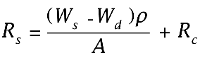
Where Ws is the thickness of the substrate, Wd is the width of the depleted region, A is the diffused area of the junction, ρ is the resistivity of the substrate and Rc is the contact resistance. Series resistance is used to determine the rise time and the linearity of the photodiode.
Junction Capacitance, C jThe boundaries of the depletion region act as the plates of a parallel plate capacitor. The junction capacitance is directly proportional to the diffused area and inversely proportional to the width of the depletion region. The capacitance is dependent on the reverse bias as follows: Where ε0 is the permittivity of free space, ε is the semiconductor dielectric constant, μ is the mobility of the majority carriers, ρ is the resistivity, Vbi is the built-in voltage of the semiconductor of the P-N junction and VA is the applied bias. Figure 1.8 shows the typical capacitance of FCI-InGaAs-500 as a function of the applied reverse bias voltage. Junction capacitance is used to determine the speed of the response of the photodiode.
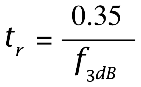
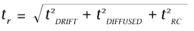
Rise/Fall time and Frequency Response, t r / t f / f 3dBThe rise time and fall time of a photodiode is defined as the time for the signal to rise or fall from 10% to 90% or 90% to 10% of the final value respectively. This parameter can be also expressed as frequency response, which is the frequency at which the photodiode output decreased by 3dB. It is roughly approximated by:
These are three factors defining the response time of a photodiode:
In a photodiode two sources of noise can be identified. Shot noise and Johnson noise.
Shot NoiseShot noise is related to the statistical fluctuation in both the photocurrent and the dark current. The magnitude of the shot noise is expressed as the root mean square (rms) noise current:
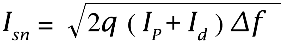
Where q=1.6x10⁻¹⁹C is the electron charge, Ip is the photogenerated current, Id is the photodetector dark current and Δf is the noise measurement bandwidth.
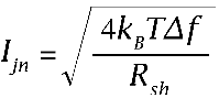
Where kB=1.38x10⁻²³J/°K, is the Boltzmann Constant, T is the absolute temperature in degrees Kelvin (273°K=0°C), Δf is the noise measurement bandwidth, and Rsh is the shunt resistance of the photodiode. This type of noise is the dominant current noise in photovoltaic (unbias) operation mode.
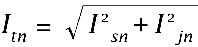
Total NoiseThe total noise current generated in a photodetector is determined by:
Noise Equivalent Power is the amount of incident light power on a photodetector, which generates a photocurrent equal to the noise current. NEP is defined as:
Where Rλ is the responsivity in A/W and Itn is the total noise of the photodetector. For InGaAs photodiodes, NEP values can vary from 10-14W/√Hz for large active area down to 10-15W/√Hz for small active area photodiodes.
TEMPERATURE EFFECTSAll photodiode characteristics are affected by changes in temperature. They include shunt resistance, dark current, breakdown voltage, and to a lesser extent other parameters such as junction capacitance.
Shunt Resistance and Dark Current:There are two major currents in a photodiode contributing to dark current and shunt resistance. Diffusion current is the dominating factor in a photovoltaic (unbiased) mode of operation, which determines the shunt resistance. It varies as the square of the temperature. In photoconductive mode (reverse biased), however, the drift current becomes the dominant current (dark current) and varies directly with temperature. Thus, change in temperature affects the photodetector more in photovoltaic mode than in photoconductive mode of operation.
In photoconductive mode the dark current may approximately double for every 10ºC increase change in temperature. And in photovoltaic mode, shunt resistance may approximately double for every 6ºC decrease in temperature. The exact change is dependent on additional parameters such as the applied reverse bias, resistivity of the substrate as well as the thickness of the substrate.
SBreakdown Voltage:For small active area devices, breakdown voltage is defined as the voltage at which the dark current becomes 10μA. Since dark current increases with temperature, therefore, breakdown voltage decreases similarly with increase in temperature.
RESPONSIVITY, RλThe responsivity of a photodiode is a measure of the sensitivity to light, and it is defined as the ratio of the photocurrent Ip to the incident light power P at a given wavelength:
In another words, it is a measure of the effectiveness of the conversion of the light power into electrical current. It varies with the wavelength of the incident light as well as applied reverse bias and temperature. Responsivity increases slightly with applied reverse bias due to improved
charge collection efficiency in photodiode. This is due to decrease or increase of the band gap, because of increase or decrease in the temperature respectively. Spectral responsivity may vary from lot to lot and it is dependent on wavelength. However, the relative variations in responsivity can be reduced to less than 1% on a selected basis.
BIASINGA photodiode signal can be measured as a voltage or a current. Current measurement demonstrates far better linearity, offset, and bandwidth performance. The generated photocurrent is proportional to the incident light power and it must be converted to voltage using a transimpedance configuration. The photodiode can be operated with or without an applied reverse bias depending on the application specific requirements. They are referred to as “Photoconductive” (biased) and “Photovoltaic” (unbiased) modes.
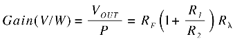
Photoconductive Mode (PC)Application of a reverse bias (i.e. cathode positive, anode negative) can greatly improve the speed of response and linearity of the devices. This is due to increase in the depletion region width and consequently decrease in junction capacitance. Applying a reverse bias, however, will increase the dark and noise currents. An example of low light level / high-speed response operated in photoconductive mode is shown in following Figure. In this configuration the detector is biased to reduce junction capacitance thus reducing noise and rise time (tr). A two stage amplification is used in this example since a high gain with a wide bandwidth is required. The two stages include a transimpedance pre-amp for current- to-voltage conversion and a non-inverting amplifier for voltage amplification. Gain and bandwidth (f3dB Max) are directly determined by RF. The gain of the second stage is approximated by 1+ R1 / R2. A feedback capacitor (CF)
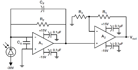
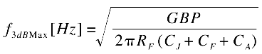
Where GBP is the Gain Bandwidth Product of amplifier (A1) and CA is the amplifier input capacitance.
In low speed applications, a large gain, e.g. >10MΩ can be achieved by introducing a large value (RF) without the need for the second stage.
In high speed, high light level measurements, however, a different approach is preferred. The most common example is pulse width measurements of short pulse gas lasers, solid state laser diodes, or any other similar short pulse light source. The photodiode output can be either directly connected to an oscilloscope or fed to a fast response amplifier. When using an oscilloscope, the bandwidth of the scope can be adjusted to the pulse width of the light source for maximum signal to noise ratio. In this application the bias voltage is large. Two opposing protection diodes should be connected to the input of the oscilloscope across the input and ground.
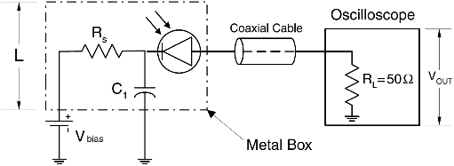
To avoid ringing in the output signal, the cable between the detector and the oscilloscope should be short (i.e. <20cm) and terminated with a 50 ohm load resistor (RL). The photodiode should be enclosed in a metallic box, if possible, with short leads between the detector and the capacitor, and between the detector and the coaxial cable. The metallic box should be tied through a capacitor (C1), with lead length (L) less than 2 cm, where RL C1> 10 t (t is the pulse width in seconds). RS is chosen such that RS