

A photosensor is an electronic component that detects the presence of visible light, infrared transmission (IR), and/or ultraviolet (UV) energy. Most photosensors consist of semiconductor having a property called photoconductivity , in which the electrical conductance varies depending on the intensity of radiation striking the material. The most common types of photosensor are the photodiode, the bipolar phototransistor, and the photoFET (photosensitive field-effect transistor). These devices are essentially the same as the ordinary diode , bipolar transistor , and field-effect transistor , except that the packages have transparent windows that allow radiant energy to reach the junctions between the semiconductor materials inside. Bipolar and field-effect phototransistors provide amplification in addition to their sensing capabilities.
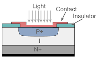
PIN Diode Basics, Working and ApplicationsThe PIN diode is a one type of photo detector, used to convert optical signal into an electrical signal. The PIN diode comprises of three regions, namely P-region, I-region and N-region. Typically, both the P and N regions are heavily doped due to they are utilized for Ohmic contacts.The intrinsic region in the diode is in contrast to a PN junction diode. This region makes the PIN diode an lower rectifier, but it makes it appropriate for fast switches, attenuators, photo detectors and applications of high voltage power electronics.
Structure and Working of PIN DiodeThe term PIN diode gets its name from the fact that includes three main layers. Rather than just having a P-type and an N-type layer, it has three layers such as
The working principle of the PIN diode exactly same as a normal diode. The main difference is that the depletion region, because that normally exists between both the P & N regions in a reverse biased or unbiased diode is larger. In any PN junction diode, the P region contains holes as it has been doped to make sure that it has a majority of holes. Likewise the N-region has been doped to hold excess electrons.
The layer between the P & N regions includes no charge carriers as any electrons or holes merge As the depletion region of the diode has no charge carriers it works as an insulator. The depletion region exists within a PIN diode, but if the PIN diode is forward biased, then the carriers come into the depletion region and as the two carrier types get together, the flow of current will starts.
When the PIN diode is connected in forward biased, the charge carriers are very much higher than the level of intrinsic carrier’s attention. Due to this reason the electric field and the high level injection level extends deeply into the region. This electric field assists in speeding up of the moving of charge carriers from P to N region, which consequences in quicker operation of the PIN diode, making it an appropriate device for high frequency operations.
The applications of PIN mainly include the following areas
At higher frequencies, PIN diode appears like an approximately perfect resistor. There is a set of stored charge in the intrinsic region. At small frequencies, the charge can be detached and the diode switched OFF.
At higher frequencies, there is not sufficient time to eliminate the charge, so the PIN diode never switched OFF. The diode has a reduced reverse recovery time. A PIN diode properly biased, therefore performs as a variable resistor. This high-frequency resistance may differ over a broad range (from 0.1 Ω-10 kΩ in some cases; the practical range is slighter, though).
The wider intrinsic area also means the PIN diode will have a low capacitance when reverse-biased. In this diode, the depletion region exists completely in the intrinsic region. This depletion region is much better than in a PN-diode, and nearly constant-size, independent of the reverse bias applied to the PN-diode.
This increases the amount where pairs of electron-hole can be produced by an occurrence photon. Some photo detector devices like photo transistors and PIN photodiodes employ a PIN-junction in their construction.
The design of the PIN-diode has some design tradeoffs. Rising the magnitudes of the intrinsic region permits the diode to appear like a resistor at minor frequencies. It harmfully affects the time required to switch off the diode & its shunt capacitance. Therefore, it is essential to choose a device with the most suitable properties for a particular use.
Integrated circuits, also known as ICs, chips, or microchips, form the basis for most of modern electronics technology. These circuits are manufactured on a single conductive piece of material, allowing them a smaller size as well as simplified design and manufacturing.
An integrated circuit, also called a chip, is an electronic circuit formed from thousands, millions, or even billions of transistors, resistors, and capacitors. It performs the same function as a larger circuit constructed using discrete (individually packaged) components, but an IC is an extremely compact device that is constructed as a single unit on a small piece of semiconducting material. The main raw material used in making an IC is silicon; hence the fact that ICs are popularly called “silicon chips.” Other raw materials like germanium and gallium arsenide may also be used, but silicon is the primary choice due to the following reasons:
An IC is designed for a purpose and can be used across various industries, such as aerospace, automotive, telecom, computers, and so on. One or more ICs, along with other components and connectors, are mounted on the printed circuit board (PCBs) and connected with thin strips of copper to cater an application. A very common use of a PCB is as the mother board of a computer.
Integrated circuit design, or IC design, is a subset of electronics engineering, encompassing the particular logic and circuit design techniques required to design integrated circuits, or ICs. ICs consist of miniaturized electronic components built into an electrical network on a monolithic semiconductor substrate by photolithography.
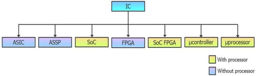
IC design can be divided into the broad categories of digital and analog IC design. Digital IC design is to produce components such as microprocessors, FPGAs, memories (RAM, ROM, and flash) and digital ASICs. Digital design focuses on logical correctness, maximizing circuit density, and placing circuits so that clock and timing signals are routed efficiently. Analog IC design also has specializations in power IC design and RF IC design. Analog IC design is used in the design of op-amps, linear regulators, phase locked loops, oscillators and active filters. Analog design is more concerned with the physics of the semiconductor devices such as gain, matching, power dissipation, and resistance. Fidelity of analog signal amplification and filtering is usually critical and as a result, analog ICs use larger area active devices than digital designs and are usually less dense in circuitry.
Design For ManufacturingDesign for manufacturing (DFM) refers to actions taken during the physical design stage of IC development to ensure that the design can be accurately manufactured.
At larger nodes, most of the defects in the IC manufacturing process were due to out-of-tolerance process steps, i.e., a macro level variation, or random particles interrupting the flow of light through a layout mask during a lithography printing step or being embedded in a layer of the wafer itself. Process control feedback loops and cleanrooms are effective in controlling these two mechanisms respectively and producing high yields.
However, as we moved from the 90nm node through 65nm, 40nm, 32nm, 28nm, 20nm and 16/14nm, the industry had expected that we would transition to EUV lithography to take advantage of shorter wavelengths for the lithography process. But due to delays in deploying EUV technology, the industry is still using light-based steppers with a wavelength of 193nm.
Diffraction effects become significant when the light interacts with objects and slits approaching the dimensions of the light wavelength. Semiconductor manufacturing has moved far beyond that threshold. From 130nm to 65nm, resolution enhancement technologies, including optical proximity correction (also referred to as computational lithography), were able to deal with the distortions caused by diffraction effects. This involves modeling the expected light distortions and making changes to the masks to correct for them so the resulting exposure on the wafer is correct as intended.
IC Desing Steps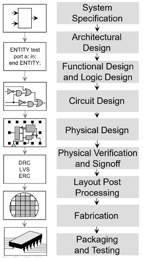
An Integrated Circuit (IC) is also called as chip or microchip. It is a semiconductor wafer in which millions of components are fabricated. The active and passive components such as resistors, diodes, transistors etc and external connections are usually fabricated in on extremely tiny single chip of silicon. All circuit components and interconnections are formed on single thin wafer (substrate) is called monolithic IC. IC is very small in size. It require microscope to see connections between components. The steps to fabricate IC chips is similar to the steps required to fabricate transistors, diodes etc. In IC chips, the fabrication of circuit elements such as transistors, diodes, capacitors etc. and their interconnections are done at same time. It has so many advantages such as extremely small size, small weight, low cost, low power consumption, .high processing speed, easy replacement, etc. IC is the principal component in all electronic devices. IC can function as amplifier, oscillator, timer, counter, computer memory etc.
Steps for IC FabricationThe manufacturing of Integrated Circuits (IC) consists of following steps. The steps includes 8-20 patterned layers created into the substrate to form the complete integrated circuit. The electrically active regions are created due to this layering in and on the surface of wafer. Hundreds of integrated circuits can be made on a single thin silicon. Then it is cut into individual IC chips.
Step 1 Wafer ProductionThe first step is wafer production. The wafer is a round slice of semiconductor material such as silicon. Silicon is preferred due to its characteristics. It is more suitable for manufacturing IC. It is the base or substrate for entire chip. First purified polycrystalline silicon is created from the sand. Then it is heated to produce molten liquid. A small piece of solid silicon is dipped on the molten liquid. Then the solid silicon (seed) is slowly pulled from the melt. The liquid cools to form single crystal ingot. A thin round wafer of silicon is cut using wafer slicer. Wafer slicer is a precise cutting machine and each slice having thickness about .01 to .025inches. When wafer is sliced, the surface will be damaged. It can be smoothening by polishing. After polishing the wafer, it must thoroughly clean and dried. The wafers are cleaned using high purity low particle chemicals .The silicon wafers are exposed to ultra pure oxygen.
Epitaxial GrowthIt means the growing of single silicon crystal upon original silicon substrate. A uniform layer of silicon dioxide is formed on the surface of wafer.
Step 2 MaskingTo protect some area of wafer when working on another area, a process called photolithography is used. The process of photolithography includes masking with a photographic mask and photo etching. A photoresist film is applied on the wafer. The wafer is aligned to a mask using photo aligner. Then it is exposed to ultraviolet light through mask. Before that the wafer must be aligned with the mask. Generally, there are automatic tools for alignment purpose.
Step 3 EtchingIt removes material selectively from the surface of wafer to create patterns. The pattern is defined by etching mask. The parts of material are protected by this etching mask. Either wet (chemical) or dry (physical) etching can be used to remove the unmasked material. To perform etching in all directions at same time, isotropic etching will be used. Anisotropic etching is faster in one direction. Wet etching is isotropic, but the etching time control is difficult. Wet etching uses liquid solvents for removing materials. It is not suited to transfer pattern with submicron feature size. It does not damage the material. Dry etching uses gases to remove materials. It is strongly anisotropic. But it is less selective. It is suited to transfer pattern having small size. The remaining photo resist is finally removed using additional chemicals or plasma. Then the wafer is inspected to make sure that the image is transferred from mask to the top layer of wafer.
Step 4 DopingTo alter the electrical character of silicon, atom with one less electron than silicon such as boron and atom with one electron greater then silicon such as phosphorous are introduced into the area. The P-type (boron) and N-type (phosphorous) are created to reflect their conducting characteristics. Diffusion is defined as the movement of impurity atoms in semiconductor material at high temperature.
Atomic diffusionIn this method p and n regions are created by adding dopants into the wafer. The wafers are placed in an oven which is made up of quartz and it is surrounded with heating elements. Then the wafers are heated at a temperature of about 1500-2200°F. The inert gas carries the dopant chemical. The dopant and gas is passed through the wafers and finally the dopant will get deposited on the wafer. This method can only be used for large areas. For small areas it will be difficult and it may not be accurate.
Ion implantationThis is also a method used for adding dopants. In this method, dopant gas such as phosphine or boron trichloride will be ionized first. Then it provides a beam of high energy dopant ions to the specified regions of wafer. It will penetrate the wafer. The depth of the penetration depends on the energy of the beam. By altering the beam energy, it is possible to control the depth of penetration of dopants into the wafer. The beam current and time of exposure is used to control the amount of dopant. This method is slower than atomic diffusion process. It does not require masking and this process is very precise. First it points the wafer that where it is needed and shoot the dopants to the place where it is required.
Step 5 MetallizationIt is used to create contact with silicon and to make interconnections on chip. A thin layer of aluminum is deposited over the whole wafer. Aluminium is selected because it is a good conductor, has good mechanical bond with silicon, forms low resistance contact and it can be applied and patterned with single deposition and etching process.
Making successive layers: - The process such as masking, etching, doping will be repeated for each successive layers until all integrated chips are completed. Between the components, silicon dioxide is used as insulator. This process is called chemical vapor deposition. To make contact pads, aluminum is deposited. The fabrication includes more than three layers separated by dielectric layers. For electrical and physical isolation a layer of solid dielectric is surrounded in each component which provides isolation. It is possible to fabricate PNP and NPN transistor in the same silicon substrate. To avoid damage and contamination of circuit, final dielectric layer (passivation) is deposited. After that, the individual IC will be tested for electrical function. Check the functionality of each chip on wafer. Those chips are not passed in the test will be rejected.
Assembly and PackagingEach of the wafers contains hundreds of chips. These chips are separated and packaged by a method called scribing and cleaving. The wafer is similar to a piece of glass. A diamond saw cut the wafer into single chips. The diamond tipped tool is used to cut the lines through the rectangular grid which separates the individual chips. The chips that are failed in electrical test are discarded. Before packaging, remaining chips are observed under microscope. The good chip is then mounted into a package. Thin wire is connected using ultrasonic bonding. It is then encapsulated for protection. Before delivered to customer, the chip is tested again. There are three configurations available for packaging. They are metal can package, ceramic flat package and dual in line package. For military applications, the chip is assembled in ceramic packages. The complete integrated circuits are sealed in anti static plastic bags.